Semicon 2.0 opens for ₹1,27,500 crore; 5 of the first 12 chip projects now produce
What the electronics ministry said on 6 November: which Semicon 2.0 pillars now take applications, how many first-round chip projects produce, and 12 new component plants.

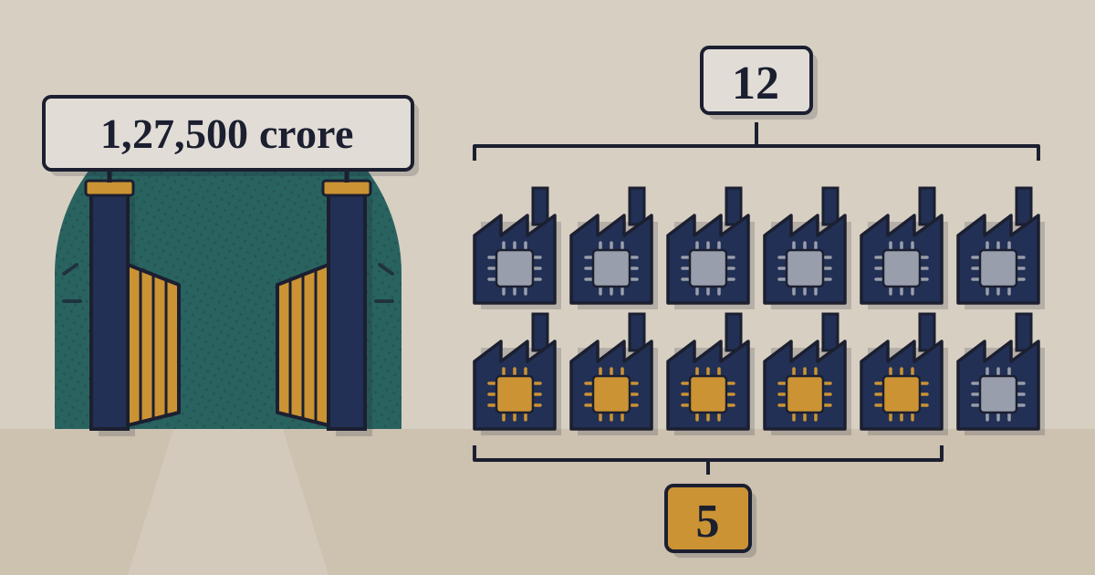
India’s second chip programme, Semicon 2.0, with a budget of ₹1,27,500 crore, began taking applications on 6 November for three of its six pillars: machines and materials, new fabs, and chip assembly and packaging. The same day the electronics ministry said 5 of the 12 chip projects approved in the first round were in commercial production as of October; those 12 carry more than ₹1.64 lakh crore of investment.1
₹1,27,500 cr
Semicon 2.0’s budget, approved by the Cabinet on 15 July
Cabinet
5 of 12
first-round chip projects in commercial production by October
MeitY
₹1.64 lakh cr
investment across the first round’s 12 projects
MeitY
₹7,503 cr
investment in 12 component plants approved the same day
MeitY
01What opened on 6 November
The Cabinet approved Semicon 2.0 on 15 July with six pillars: chip design; machines and materials; more fabs; assembly and packaging, known as ATMP or OSAT; research; and talent.2 A fab prints circuits onto silicon wafers; an ATMP unit cuts the wafers into chips, then packages and tests them. The machines-and-materials pillar offers incentives to companies that make the equipment, chemicals and gases fabs consume.2 The portal opened for pillars 2, 3 and 4, and the minister, Ashwini Vaishnaw, set a target of at least three major equipment makers and five chemicals and gases companies.1 Neither release gives the support rates or a closing date for applications.
02Which of the first 12 produce
The first round approved one silicon fab, one silicon carbide fab, a gallium nitride micro-LED display fab and nine packaging units; the first fab is scheduled to be commissioned in 2028. In July the Cabinet named three companies in commercial production, Micron, Kaynes and CG Semi, and expected one more in 2026.2 By October the count was five; the November release does not name the other two.1 On design, 24 start-ups have received funding and 105 have access to chip-design software; 70,000 students at 332 institutions have been trained on it.1
03The component plants approved the same day
Under a separate scheme for electronic components, ECMS, the ministry approved 12 more applications: ₹7,503 crore of investment, ₹39,045 crore of projected production and 7,127 direct jobs across seven states. They include the scheme’s first approvals for copper foil, an input for circuit-board laminates and lithium-ion cells (Indo Asia Copper), cathode active material (Vidyuta Materials) and specialty ceramics (Voltix Semicon). Multi-layer circuit boards went to NeST ICELR, and factory-automation equipment to Rockwell Automation India and Wipro Pari Robotics.1 ECMS now counts 118 approvals: ₹77,051 crore of investment, ₹5,73,146 crore of projected production and 81,755 jobs, across 34 products and 16 states.1
What to watch: the names of the two newest producers, the support rates for the second round, and the first fab’s 2028 date. How the world’s largest chip maker’s sales are running is in our TSMC monthly-revenue Trend.
Sources
- Ministry of Electronics and IT (PIB): Union Minister Ashwini Vaishnaw launches Semicon 2.0 web application portal and announces 12 approved applicants under ECMS — 6 November 2026
- Cabinet: Cabinet approves Semicon 2.0 (PM India) — 15 July 2026
- Cabinet (PIB): Programme for development of semiconductors and display manufacturing ecosystem in India, ₹76,000 crore — 15 December 2021
Disclosure. TechBag is a software reseller: it earns when companies buy through it, including from vendors named here. The analysis is TechBag’s own; no vendor paid for or saw this piece before publication. Facts are labelled reported, TechBag count or our view.
Keep reading